In an era when the electronics industry was dominated by vacuum tubes and mechanical relays, one engineer had the audacity to imagine a future lit by tiny, luminous crystals. Nick Holonyak Jr. didn’t just predict that future — he built it. In 1962, working at a General Electric lab in Syracuse, New York, he created the first practical visible-spectrum light-emitting diode (LED), a device that would eventually reshape lighting, displays, telecommunications, and energy consumption worldwide. Today, LEDs illuminate everything from smartphone screens to stadium floodlights, saving billions of kilowatt-hours annually. It all started with a man who believed semiconductors could do far more than switch circuits — they could generate light visible to the human eye.
Early Life and Education
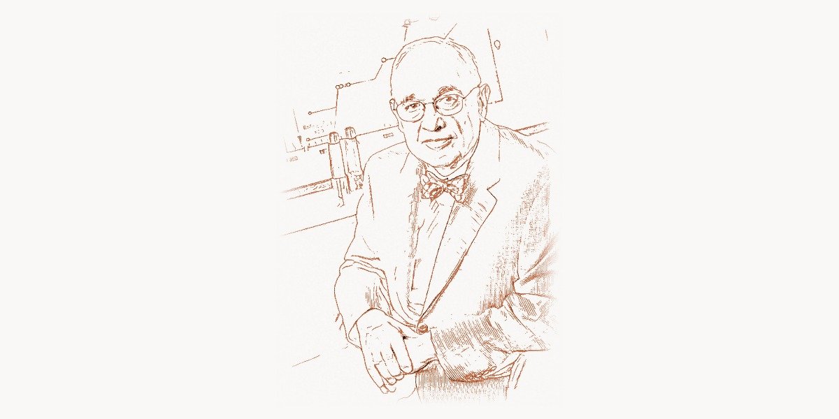
Nick Holonyak Jr. was born on November 3, 1928, in Zeigler, Illinois, a small coal-mining town in the southern part of the state. His father, Nick Holonyak Sr., was an immigrant from the Carpathian region who worked in the local mines. The family lived modestly, and young Nick grew up acutely aware of the physical toll that manual labor extracted from workers like his father. That awareness planted a seed: he resolved early on that education would be his path out of the mines.
Holonyak attended the University of Illinois at Urbana-Champaign, where he earned his bachelor’s degree in electrical engineering in 1950, followed by a master’s degree in 1951. He then pursued doctoral studies under John Bardeen — the only person to have won two Nobel Prizes in Physics (for the transistor in 1956 and superconductivity theory in 1972). Being mentored by Bardeen was transformative. Holonyak absorbed not just technical expertise in semiconductor physics, but a philosophical approach to research: pursue fundamental understanding, and applications will follow. He completed his Ph.D. in electrical engineering in 1954, becoming one of Bardeen’s first doctoral students at Illinois.
The mentorship under Bardeen connected Holonyak to the very origin of the transistor revolution. While peers like Jack Kilby and Robert Noyce would soon miniaturize transistors into integrated circuits, Holonyak was drawn to a different frontier: the light-emitting properties of compound semiconductors.
Career and the Invention of the Visible LED
Technical Innovation: Making Semiconductors Glow
After completing his doctorate, Holonyak joined Bell Labs briefly before moving to the U.S. Army Signal Corps laboratory, where he worked on semiconductor devices. In 1957, he joined General Electric’s Advanced Semiconductor Laboratory in Syracuse, New York. It was there that his most consequential work began.
At the time, researchers knew that certain semiconductor materials could emit light — a phenomenon called electroluminescence. In 1961, Robert Biard and Gary Pittman at Texas Instruments had created an infrared LED using gallium arsenide (GaAs). But infrared light is invisible to the human eye, limiting its practical applications to photodetectors and remote controls.
Holonyak took a fundamentally different approach. Instead of pure gallium arsenide, he experimented with gallium arsenide phosphide (GaAsP), a ternary compound semiconductor. By carefully adjusting the ratio of arsenic to phosphorus in the crystal lattice, he could tune the bandgap energy — the gap between a semiconductor’s valence band and conduction band — to a level that corresponded to visible-light wavelengths. The physics can be expressed simply:
# Simplified bandgap-to-wavelength relationship for LEDs
# E_g (bandgap energy in eV) determines the wavelength of emitted photons

PLANCK_CONSTANT = 4.1357e-15   # eV·s
SPEED_OF_LIGHT = 3e8           # m/s

def bandgap_to_wavelength_nm(bandgap_ev):
    """Convert bandgap energy to emitted photon wavelength in nanometers."""
    wavelength_m = (PLANCK_CONSTANT * SPEED_OF_LIGHT) / bandgap_ev
    return wavelength_m * 1e9  # convert to nm

# GaAs (infrared LED) — bandgap ~1.42 eV
infrared_wavelength = bandgap_to_wavelength_nm(1.42)
print(f"GaAs LED: {infrared_wavelength:.0f} nm (infrared, invisible)")

# GaAsP (Holonyak's visible LED) — bandgap ~1.9 eV
visible_wavelength = bandgap_to_wavelength_nm(1.9)
print(f"GaAsP LED: {visible_wavelength:.0f} nm (red, visible!)")

# GaN (modern blue LED) — bandgap ~3.4 eV
blue_wavelength = bandgap_to_wavelength_nm(3.4)
print(f"GaN LED: {blue_wavelength:.0f} nm (blue/violet)")
By pushing the phosphorus content higher in the GaAsP alloy, Holonyak widened the bandgap enough that recombining electrons and holes emitted red photons at approximately 710 nm — right at the edge of human-visible light. On October 9, 1962, his device glowed red. It was the first practical visible-spectrum LED.
The achievement was reported in the December 1962 issue of Applied Physics Letters. General Electric promoted the invention, and Holonyak was featured in Reader’s Digest in 1963, where he made a bold prediction: LEDs would eventually replace Thomas Edison’s incandescent light bulb. At the time, most dismissed the claim as fantasy — his LED emitted a feeble reddish glow. But Holonyak understood the trajectory of semiconductor technology better than most.
Why It Mattered: From Indicator Light to Global Illumination
The visible LED didn’t just add a color option to existing infrared technology. It unlocked entirely new categories of application. The first visible LEDs appeared as indicator lights on circuit boards and instrument panels. But the real significance was that Holonyak had demonstrated a principle: by engineering compound semiconductors, you could control the color of emitted light. This opened the door for other researchers to develop orange, yellow, and eventually green LEDs in the 1970s.
The final piece of the puzzle — the blue LED — took another three decades, eventually achieved by Isamu Akasaki, Hiroshi Amano, and Shuji Nakamura using gallium nitride (GaN) in the early 1990s. Their work earned the 2014 Nobel Prize in Physics. But every step on that journey followed the path Holonyak had blazed: tune the bandgap, change the light.
Today, LEDs account for more than half of global lighting sales. They consume up to 90% less energy than incandescent bulbs and last 25 times longer. In displays, LED and OLED technology powers everything from NVIDIA GPUs driving monitors to the screens on every smartphone. The economic impact is measured in hundreds of billions of dollars annually. And it all traces back to a small red glow in a Syracuse lab — the work of a coal miner’s son who studied under a Nobel laureate.
Other Contributions
While the visible LED remains Holonyak’s signature achievement, his career was remarkably prolific. He made foundational contributions in several other areas of semiconductor technology:
- Quantum-well laser — In the 1970s and 1980s, Holonyak and his students pioneered the development of quantum-well heterostructure lasers. These devices confine electrons within ultra-thin semiconductor layers, producing laser light far more efficiently than bulk semiconductor lasers. Quantum-well lasers became the foundation for fiber-optic communications, CD/DVD players, and barcode scanners — technologies that reshaped how the world stores and transmits information.
- Laser diode advancements — He contributed to the development of the first semiconductor laser diodes that could operate continuously at room temperature, eliminating the need for cryogenic cooling. This breakthrough was essential for practical deployment in telecommunications, where engineers like Vint Cerf and Bob Kahn were building the network infrastructure that relied on fiber optics.
- Transistor dimmer switch — Holonyak invented the first semiconductor dimmer switch, replacing bulky rheostats with compact solid-state circuits. This seemingly modest invention became ubiquitous in homes and commercial buildings worldwide.
- Shockley diode and PNPN devices — Early in his career at GE, Holonyak worked on four-layer semiconductor switches (thyristors), contributing to the development of power electronics that control everything from industrial motors to power grid systems.
His work on quantum-well lasers alone would have secured a distinguished legacy. These devices are direct ancestors of the lasers that carry internet traffic through fiber-optic cables — the same cables that enable the digital infrastructure companies like Toimi rely on to deliver modern web solutions.
Philosophy and Approach to Innovation
Holonyak’s approach to research was shaped by two powerful influences: the practical, no-nonsense work ethic he absorbed growing up in a mining community, and the rigorous intellectual discipline he learned from John Bardeen. He was not a theoretician who waited for elegant mathematics to guide him — he was an experimentalist who built things and observed what happened. But neither was he a tinkerer without depth. He insisted on understanding the fundamental physics before attempting to engineer a device.
In a field where researchers often chased incremental improvements, Holonyak consistently aimed at problems others considered unsolvable. When colleagues at GE told him that visible-light emission from semiconductors was impractical, he ignored them and kept experimenting with GaAsP alloys. When others dismissed LEDs as novelty indicators, he predicted they would replace the incandescent bulb.
Key Principles
- Start from fundamentals — Holonyak believed that understanding semiconductor physics at the atomic level was prerequisite to any meaningful engineering. He did not treat devices as black boxes.
- Material science is destiny — He recognized earlier than most that the choice of semiconductor material determined what a device could do. His career was built on exploring new materials (GaAsP, AlGaAs, InGaP) rather than optimizing existing ones.
- Mentor relentlessly — Over his 50+ year academic career, Holonyak supervised more than 60 doctoral students, many of whom went on to lead semiconductor research at major universities and companies. He viewed teaching as inseparable from research.
- Think in decades — His 1963 prediction that LEDs would replace the light bulb was vindicated half a century later. He understood that semiconductor technology followed exponential improvement curves, much like the trajectory Gordon Moore formalized for transistor density.
- Build, don’t just theorize — Holonyak insisted on hands-on fabrication. He grew his own semiconductor crystals, built his own devices, and tested them himself. This direct engagement with materials gave him intuitions that purely theoretical researchers lacked.
This combination of deep physics knowledge and relentless experimental drive made Holonyak extraordinarily productive. His publication record spans hundreds of papers, and his students carried his methods into labs around the world.
// LED evolution timeline — from Holonyak's first red LED to modern lighting
const ledMilestones = [
  { year: 1962, event: "Nick Holonyak Jr. creates first visible (red) LED", material: "GaAsP", color: "Red" },
  { year: 1968, event: "First commercial LED indicator lights ship", material: "GaAsP", color: "Red" },
  { year: 1972, event: "M. George Craford (Holonyak's student) creates yellow LED", material: "GaAsP:N", color: "Yellow" },
  { year: 1976, event: "High-brightness red/orange LEDs become affordable", material: "AlGaAs", color: "Red/Orange" },
  { year: 1993, event: "Nakamura demonstrates first bright blue LED", material: "InGaN", color: "Blue" },
  { year: 1996, event: "White LED created using blue LED + phosphor", material: "InGaN + YAG", color: "White" },
  { year: 2006, event: "LED efficacy surpasses incandescent bulbs", material: "Various", color: "White" },
  { year: 2014, event: "Blue LED inventors receive Nobel Prize in Physics", material: "GaN", color: "Blue" },
  { year: 2024, event: "LEDs represent >50% of global lighting market", material: "Various", color: "All" },
];

ledMilestones.forEach(m => {
  const milestone = `${m.year}: [${m.color}] ${m.event} (${m.material})`;
  console.log(milestone);
});

// Holonyak's student M. George Craford alone holds
// over 40 patents in LED technology — a testament to
// the impact of Holonyak's mentorship pipeline
Legacy and Recognition
Nick Holonyak Jr. returned to the University of Illinois at Urbana-Champaign in 1963, where he became the John Bardeen Endowed Chair Professor — a fitting title given his doctoral lineage. He remained at Illinois for over five decades, continuing research and mentoring generations of semiconductor engineers until his retirement.
His honors are extensive and reflect the breadth of his impact:
- National Medal of Science (1990) — awarded by President George H.W. Bush
- National Medal of Technology and Innovation (2002) — awarded by President George W. Bush, making Holonyak one of very few individuals to receive both national medals
- IEEE Edison Medal (1989)
- Japan Prize (1995) — for his contributions to LED and laser technology
- Lemelson-MIT Prize (2004)
- Induction into the National Inventors Hall of Fame (2008)
- Over 500 published papers and more than 40 patents
His students form a notable lineage of their own. M. George Craford, who studied under Holonyak, went on to develop high-brightness yellow and red LEDs and is considered the most prolific LED researcher in history. Russell Dupuis, another Holonyak student, advanced metalorganic chemical vapor deposition (MOCVD), the manufacturing technique that made mass production of LEDs and laser diodes possible.
Holonyak passed away on September 18, 2022, at the age of 93, in Urbana, Illinois. His death was widely mourned in the engineering community, with the University of Illinois calling him one of the most important alumni in its history. The LED lighting revolution he ignited continues to accelerate — modern research into micro-LEDs, UV LEDs for sterilization, and LiFi (light-based wireless communication) all descend from the principles he established.
In a broader context, Holonyak’s work sits alongside the achievements of other hardware pioneers who transformed abstract physics into everyday technology. Just as Federico Faggin turned semiconductor theory into the first commercial microprocessor, and Sophie Wilson designed the energy-efficient ARM architecture that powers billions of devices, Holonyak turned the physics of electroluminescence into a technology that now lights the world. Teams building modern digital products — whether through platforms like Taskee or custom development pipelines — ultimately depend on the hardware foundation that innovators like Holonyak created.
Key Facts About Nick Holonyak Jr.
- Born: November 3, 1928, in Zeigler, Illinois
- Died: September 18, 2022, in Urbana, Illinois (age 93)
- Education: B.S. (1950), M.S. (1951), Ph.D. (1954) in Electrical Engineering, University of Illinois at Urbana-Champaign
- Doctoral advisor: John Bardeen (two-time Nobel Prize winner in Physics)
- Key invention: First practical visible-spectrum LED (1962) using gallium arsenide phosphide
- Material innovation: Demonstrated that ternary compound semiconductors (GaAsP) could be engineered to emit visible light
- Career: General Electric (1957–1963), University of Illinois (1963–2013)
- Awards: National Medal of Science, National Medal of Technology and Innovation, Japan Prize, IEEE Edison Medal, Lemelson-MIT Prize
- Mentorship: Supervised 60+ doctoral students, including LED pioneer M. George Craford
- Patents: Over 40 granted patents in semiconductor devices
- Legacy: LEDs now account for over 50% of global lighting, saving billions in energy costs annually
Frequently Asked Questions
What exactly did Nick Holonyak Jr. invent?
Holonyak invented the first practical visible-spectrum light-emitting diode (LED) in 1962. While infrared (invisible) LEDs existed before his work, Holonyak was the first to create an LED that emitted light the human eye could see — specifically, red light at approximately 710 nm wavelength. He achieved this by using gallium arsenide phosphide (GaAsP), a compound semiconductor whose bandgap he engineered to produce visible photons. This single breakthrough opened the door to the entire modern LED industry, from indicator lights to room illumination.
Why didn’t Nick Holonyak Jr. win the Nobel Prize for the LED?
The 2014 Nobel Prize in Physics was awarded to Isamu Akasaki, Hiroshi Amano, and Shuji Nakamura for the blue LED, which was the final missing piece needed to produce white LED light (by combining blue LEDs with yellow phosphor coatings). The Nobel Committee emphasized that blue LEDs enabled practical white lighting, which had the greatest energy-saving impact. Many in the scientific community — including the blue LED laureates themselves — have acknowledged that Holonyak’s 1962 red LED was the foundational invention. Holonyak did receive both the National Medal of Science and the National Medal of Technology and Innovation, the two highest U.S. honors for scientific and technological achievement.
How did Holonyak’s mentorship under John Bardeen influence his career?
John Bardeen, Holonyak’s doctoral advisor, co-invented the transistor and later developed the BCS theory of superconductivity — earning Nobel Prizes for both. Under Bardeen, Holonyak learned to approach semiconductor research from first principles rather than trial-and-error. Bardeen’s emphasis on understanding quantum mechanics and solid-state physics at a deep level gave Holonyak the theoretical foundation to recognize that compound semiconductors like GaAsP could be engineered to emit visible light. Holonyak often credited Bardeen with teaching him how to think about problems, not just how to solve them. Much as Claude Shannon built information theory on deep mathematical foundations, Holonyak built his experimental program on rigorous physics.
What is the connection between Holonyak’s LED and modern display technology?
Every modern LED display — from smartphone OLED screens to massive stadium video walls — descends from the principle Holonyak demonstrated in 1962: that semiconductors can be engineered to emit specific colors of visible light. His red LED was the first proof of concept. Subsequent researchers developed green and blue LEDs, completing the RGB (red-green-blue) triad needed for full-color displays. Modern micro-LED displays, which companies like Apple and Samsung are developing as successors to OLED, use arrays of microscopic LEDs to create pixels — each one a direct descendant of Holonyak’s original invention. The display industry, which now exceeds $150 billion annually, rests on the foundation he built.