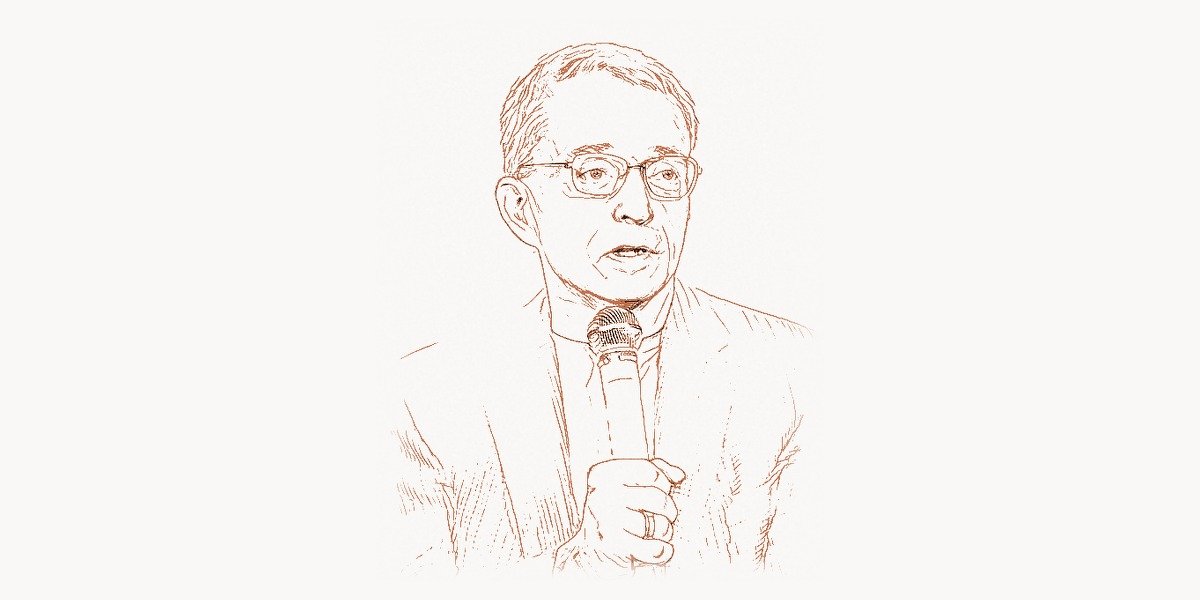
In the annals of Silicon Valley, few careers arc as dramatically as that of Pat Gelsinger. At just 32 years old, he became the youngest vice president in Intel’s history — a title earned not through corporate maneuvering but through raw technical brilliance and an obsessive dedication to the craft of chip design. Decades later, after steering VMware through a cloud revolution and returning to Intel as CEO during one of its most turbulent chapters, Gelsinger would attempt something most industry observers considered impossible: rebuilding Intel’s manufacturing dominance through an ambitious foundry strategy. Whether history will judge that gamble a success or a premature vision, one thing is undeniable — Pat Gelsinger shaped the semiconductor industry at every level, from transistor architecture to corporate strategy.
Early Life and Education
Patrick Paul Gelsinger was born on April 5, 1961, in Robesonia, Pennsylvania — a small town in Berks County with a population barely crossing four figures. He grew up on a family farm, the son of a butcher, in a household that valued hard work and faith far more than technology. Nothing in his early environment suggested he would one day lead one of the most important technology companies on the planet.
Gelsinger’s introduction to electronics came through a vocational technology program at his local high school, where he discovered an aptitude for circuits and logic that set him apart from his peers. The program connected him to a co-op job at a small electronics firm, which in turn opened the door to Lincoln Technical Institute, where he earned an associate degree in electrical technology in 1979.
What happened next changed the trajectory of his life. At 18, Gelsinger joined Intel as a quality control technician — one of the lowest rungs on the engineering ladder. But he was hungry. While working full-time at Intel, he pursued his bachelor’s degree in electrical engineering from Santa Clara University, followed by a master’s degree from Stanford University. He would later earn a master’s in engineering management from Stanford as well. This pattern — relentless self-improvement while delivering results on the job — became the defining rhythm of his entire career.
His early mentors at Intel recognized something exceptional. Andy Grove, Intel’s legendary CEO, took a personal interest in Gelsinger’s development, assigning him increasingly challenging roles. Grove saw in the young engineer the same intensity and intellectual rigor that had defined Intel’s early culture, and he invested heavily in Gelsinger’s growth as both a technologist and a leader.
Career and the Intel Foundry Vision
Technical Innovation: From 486 to IDM 2.0
Gelsinger’s technical credentials are not abstract or honorary — they were forged in the trenches of silicon design. He served as the lead architect of the Intel 486 processor, the chip that brought true multitasking capability to personal computing in 1989. The 486 integrated a floating-point unit, cache, and pipelined architecture onto a single die — a feat that represented a generational leap in x86 design. The chip contained 1.2 million transistors, implementing concepts that would define PC architecture for years to come.
To appreciate the significance of the 486, consider the context. At the time, Gordon Moore’s famous law was the guiding principle of the semiconductor industry, and the 486 was one of the chips that proved it could keep going. Gelsinger didn’t just follow Moore’s Law — he engineered one of its most convincing validations. The chip’s pipelined integer unit could be modeled conceptually as a staged processing chain:
# Simplified 5-stage pipeline model inspired by 486 architecture
class PipelineStage:
    def __init__(self, name, latency_cycles=1):
        self.name = name
        self.latency = latency_cycles
        self.instruction = None

    def process(self, instruction):
        self.instruction = instruction
        return f"{self.name}: processing {instruction}"

class IntelPipeline:
    """Model of the 486's 5-stage integer pipeline"""
    def __init__(self):
        self.stages = [
            PipelineStage("Fetch"),
            PipelineStage("Decode1"),
            PipelineStage("Decode2"),
            PipelineStage("Execute"),
            PipelineStage("WriteBack")
        ]

    def throughput_improvement(self, instructions, baseline_cycles=5):
        """Calculate pipeline speedup vs non-pipelined execution"""
        n = len(instructions)
        pipelined_cycles = baseline_cycles + (n - 1)
        sequential_cycles = n * baseline_cycles
        speedup = sequential_cycles / pipelined_cycles
        return {
            "pipelined_cycles": pipelined_cycles,
            "sequential_cycles": sequential_cycles,
            "speedup_factor": round(speedup, 2)
        }

# With 100 instructions, pipeline approaches 5x throughput
pipeline = IntelPipeline()
result = pipeline.throughput_improvement(list(range(100)))
print(f"Speedup: {result['speedup_factor']}x")  # ~4.81x
After the 486, Gelsinger rose through Intel’s ranks with remarkable speed, becoming the company’s first Chief Technology Officer in 2001. In this role, he oversaw Intel’s technology direction across all product lines, from server chips to mobile processors. His technical vision encompassed not just processor architecture but the entire platform ecosystem — a holistic view that would prove prescient in the era of heterogeneous computing.
But it was his return to Intel as CEO in February 2021 that defined his most ambitious chapter. Intel was in crisis. Years of manufacturing delays had cost the company its process leadership to TSMC and Samsung. Competitors like AMD under Lisa Su were eating into Intel’s market share with chips manufactured at TSMC’s cutting-edge nodes. NVIDIA under Jensen Huang had redefined the computing landscape with GPU-accelerated AI.
Gelsinger’s response was IDM 2.0 — a fundamental reimagining of Intel’s business model. The strategy had three pillars: first, accelerate Intel’s internal process technology to regain leadership by 2025 with five nodes in four years; second, open Intel’s fabs to external customers through Intel Foundry Services (IFS); and third, selectively use external foundries for some Intel products. This was revolutionary for a company that had defined the Integrated Device Manufacturer model for half a century.
Why It Mattered: The Geopolitics of Silicon
Gelsinger’s foundry strategy wasn’t just a corporate turnaround plan — it was a geopolitical statement. By 2021, roughly 92% of the world’s most advanced semiconductors were manufactured in Taiwan, creating a concentration of strategic capability that military and economic analysts called the “silicon shield.” Gelsinger recognized that Intel’s foundry ambitions aligned with a critical national security imperative: bringing advanced chip manufacturing back to American and European soil.
He secured over $50 billion in commitments for new fabrication facilities in Ohio, Arizona, Germany, and Israel. He lobbied aggressively for the CHIPS and Science Act, which eventually passed in 2022 with $52.7 billion in funding for domestic semiconductor manufacturing. Gelsinger became the public face of the argument that semiconductor manufacturing sovereignty was as important as energy independence.
The technical challenge was staggering. Intel had to simultaneously execute on EUV lithography adoption, develop new transistor architectures (RibbonFET and PowerVia), and build entirely new fabrication complexes — all while competing with TSMC’s years of momentum. The node naming itself was restructured, moving from Intel’s conservative naming to a more market-aligned scheme: Intel 7, Intel 4, Intel 3, Intel 20A, and Intel 18A.
// Intel's IDM 2.0 process roadmap visualization model
const intelProcessNodes = [
  { name: "Intel 7",  year: 2021, transistorTech: "FinFET Enhanced", nmEquiv: 10 },
  { name: "Intel 4",  year: 2022, transistorTech: "EUV FinFET",     nmEquiv: 7  },
  { name: "Intel 3",  year: 2023, transistorTech: "EUV FinFET+",    nmEquiv: 5  },
  { name: "Intel 20A", year: 2024, transistorTech: "RibbonFET + PowerVia", nmEquiv: 3 },
  { name: "Intel 18A", year: 2025, transistorTech: "RibbonFET Gen2", nmEquiv: 2 }
];

function calculateNodeProgression(nodes) {
  const results = nodes.map((node, i) => {
    const densityGain = i > 0
      ? ((nodes[i-1].nmEquiv / node.nmEquiv) ** 2).toFixed(1)
      : "baseline";
    return {
      node: node.name,
      year: node.year,
      architecture: node.transistorTech,
      relativeDensityGain: densityGain
    };
  });
  return results;
}

const roadmap = calculateNodeProgression(intelProcessNodes);
console.table(roadmap);
// Intel 18A targets ~2.5x density vs Intel 3
Whether Intel will ultimately execute on this vision remains an open question. Gelsinger departed as CEO in December 2024 amid board pressure and continued financial challenges. But the infrastructure investments he championed — the fabs, the CHIPS Act funding, the foundry customer pipeline — represent a structural shift in the global semiconductor landscape that will play out over the next decade regardless of who leads the company.
Other Contributions
Before his second stint at Intel, Gelsinger spent eight years as CEO of VMware (2012-2021), where he transformed the company from a virtualization vendor into a comprehensive cloud infrastructure platform. Under his leadership, VMware’s revenue roughly doubled, and the company expanded into network virtualization (NSX), storage virtualization (vSAN), and Kubernetes-based container orchestration (Tanzu).
VMware’s evolution under Gelsinger mirrored a broader industry shift. The same year he joined VMware, Solomon Hykes was building Docker, and the container revolution was beginning. Rather than treating containers as a competitive threat to virtual machines, Gelsinger positioned VMware as a platform that could orchestrate both — a pragmatic approach that kept VMware relevant as cloud-native architectures proliferated.
Gelsinger also played a significant role in Intel’s early USB development. As a senior engineer in the 1990s, he was involved in the platform architecture decisions that led to USB becoming a universal standard — work that intersected with the efforts of engineers like Ajay Bhatt, who is widely credited as the father of USB. Gelsinger’s platform-level thinking helped ensure that USB was not just a connector specification but an integral part of the PC architecture.
His contributions to Intel’s server and data center strategy were equally important. Gelsinger championed the Xeon processor line and helped architect Intel’s dominance in the data center market — a position that generated enormous profits for decades and funded the company’s R&D investments. His understanding of both silicon design and enterprise computing made him uniquely qualified to bridge the gap between chip architecture and customer needs.
Beyond his corporate roles, Gelsinger has been a vocal advocate for STEM education and workforce development. He has argued consistently that the semiconductor industry’s biggest constraint is not capital or technology but talent — and that the United States needs to dramatically expand its pipeline of engineers and technicians to support domestic manufacturing ambitions. His perspective on talent development aligns with the broader industry challenge that companies like Toimi address through technology-driven approaches to organizational efficiency.
Philosophy and Leadership Approach
Key Principles
- Technology leadership is non-negotiable. Gelsinger consistently argued that Intel’s identity was inseparable from process technology leadership. “If you can’t make leading-edge chips, you can’t be Intel,” was the essence of his position. This conviction drove the aggressive five-nodes-in-four-years roadmap, even when financial markets punished the spending required.
- Vertical integration is a strategic advantage, not a legacy burden. While the industry trend was toward fabless design (exemplified by AMD’s 2009 spin-off of GlobalFoundries), Gelsinger doubled down on Intel’s integrated model. He believed that owning both design and manufacturing created feedback loops that fabless competitors could never replicate — insights from manufacturing informing design, and design requirements pushing manufacturing capabilities.
- Execution velocity over perfection. Gelsinger inherited an Intel culture that had become cautious and bureaucratic after years of delays. He pushed for faster decision-making and accepted that some bets would fail. The IDM 2.0 strategy was itself a calculated risk — opening Intel’s fabs to competitors’ designs was culturally anathema to many Intel veterans.
- Geopolitical awareness is a business imperative. Long before the CHIPS Act became law, Gelsinger was sounding alarms about semiconductor supply chain concentration in East Asia. He understood that Intel’s business strategy could not be separated from national security considerations — a perspective that Jim Keller, another legendary chip architect, also brought to discussions about the future of semiconductor design.
- Faith and purpose drive sustained excellence. Unlike many Silicon Valley executives, Gelsinger has been openly and deeply religious throughout his career. He has spoken publicly about the role of faith in his leadership, including decisions to prioritize family and spiritual life alongside professional ambitions. This aspect of his character set him apart in an industry often defined by secular techno-utopianism.
- Engineer-leaders outperform manager-leaders in deep tech. Gelsinger was suspicious of leaders who couldn’t understand the technology they were directing. His own career — from 486 architect to CTO to CEO — embodied the principle that the best technology leaders are practitioners first. He could review a chip design with the same fluency that he could present a quarterly earnings call.
Legacy and Impact
Pat Gelsinger’s legacy is complex and still unfolding. His tenure as Intel CEO was marked by bold vision and painful financial realities. The stock price declined significantly during his leadership as investors grew impatient with the massive capital expenditures required by the foundry strategy. His departure in December 2024 was widely interpreted as a board losing confidence in the pace of execution.
Yet the assets he built — new fabs in Ohio and Arizona, the Intel 18A process technology, foundry customer agreements, CHIPS Act funding — represent genuine strategic value that will take years to fully materialize. In the semiconductor industry, where new fabrication facilities take three to five years to build and another two to three years to reach mature yields, Gelsinger’s investments were inherently long-horizon bets.
His earlier legacy is more clearly established. The 486 processor helped democratize personal computing. His CTO tenure guided Intel through the transition from single-core to multi-core architectures. His VMware years proved that a hardware-oriented engineer could successfully lead a software company through a major platform transition. Each chapter of his career demonstrated a capacity for reinvention that is rare in the technology industry.
In the broader narrative of the semiconductor industry, Gelsinger stands alongside figures like Federico Faggin and Morris Chang as someone who shaped not just products but the structure of the industry itself. Faggin created the microprocessor at Intel. Chang created the foundry model at TSMC. Gelsinger attempted to fuse these two legacies — building a company that could both design and manufacture leading-edge chips while also serving as a foundry for others. Whether that synthesis proves viable will be one of the defining questions of the semiconductor industry’s next decade.
For organizations navigating their own complex technological transformations, Gelsinger’s career offers a master class in the interplay between technical depth and strategic vision — the kind of integrated thinking that platforms like Taskee help teams operationalize through structured project management and collaboration tools.
Key Facts About Pat Gelsinger
- Born April 5, 1961, in Robesonia, Pennsylvania
- Joined Intel at age 18 as a quality control technician in 1979
- Lead architect of the Intel 486 processor (1989), which contained 1.2 million transistors
- Became the youngest vice president in Intel’s history at age 32
- Served as Intel’s first Chief Technology Officer (2001-2009)
- CEO of VMware from 2012 to 2021, roughly doubling the company’s revenue
- Returned as Intel CEO in February 2021 and launched the IDM 2.0 strategy
- Holds eight patents in VLSI design, processor architecture, and computer systems
- Lobbied for the CHIPS and Science Act, which allocated $52.7 billion for domestic semiconductor manufacturing
- Committed over $50 billion in new fab investments across Ohio, Arizona, Germany, and Israel
- Departed Intel as CEO in December 2024
- Holds degrees from Lincoln Technical Institute, Santa Clara University, and Stanford University
Frequently Asked Questions
What was Pat Gelsinger’s most important technical contribution?
Gelsinger’s most significant hands-on technical achievement was serving as lead architect of the Intel 486 processor. Released in 1989, the 486 was the first x86 chip to integrate a floating-point unit, cache memory, and a pipelined integer execution unit on a single die. This integration eliminated the need for separate math coprocessors and made true multitasking practical on personal computers. The 486’s architecture influenced x86 design for generations and established several concepts — on-die cache, integrated FPU, pipelined execution — that remain fundamental to modern processors.
Why did Pat Gelsinger leave Intel as CEO?
Gelsinger departed Intel in December 2024 under pressure from the board of directors. While the IDM 2.0 foundry strategy he championed was conceptually bold, the financial burden of simultaneous multi-billion-dollar fab construction projects, combined with market share losses to AMD and NVIDIA, created significant investor concern. Intel’s stock declined substantially during his tenure. The board ultimately concluded that the pace of execution on the foundry transformation was insufficient given competitive pressures, though many industry analysts noted that semiconductor manufacturing turnarounds inherently require longer timelines than Gelsinger was given.
How did Gelsinger’s VMware tenure prepare him for the Intel CEO role?
Gelsinger’s eight years at VMware (2012-2021) expanded his leadership capabilities in several critical ways. He learned to manage a large-scale software business, navigate cloud platform transitions, and execute acquisitions that repositioned a company’s strategic direction. At VMware, he also developed relationships with enterprise customers and cloud providers that proved valuable when pitching Intel Foundry Services. Perhaps most importantly, VMware taught him that legacy technology companies could reinvent themselves — a lesson he carried into his attempt to transform Intel from a product company into a product-plus-foundry company.
What is Intel Foundry Services and why was it controversial?
Intel Foundry Services (IFS) was the centerpiece of Gelsinger’s IDM 2.0 strategy — a division that would manufacture chips designed by other companies using Intel’s fabrication technology. This was revolutionary because Intel had historically manufactured only its own designs, treating its fabs as a competitive moat rather than a service. Opening the fabs to external customers meant potentially manufacturing chips for competitors, which was culturally jarring for many Intel employees and executives. The controversy extended to financial markets, where analysts debated whether Intel could simultaneously catch up on process technology, build new fabs, and develop the customer service capabilities required to compete with TSMC’s decades of foundry experience.